Sensing and controlling microscopic spin density in materials is a key aspect of spintronics, which seeks to exploit electrons’ intrinsic spin in addition to their fundamental electronic charge. Spintronics has a wide range of potential applications, including data storage, information processing, and even quantum computing.
Electronic devices typically use electron charge, but spin, their other degree of freedom, is beginning to be used. Crystalline materials with spin defects are extremely useful for quantum-based devices such as ultrasensitive quantum sensors, quantum memory devices, and systems for simulating the physics of quantum effects. Varying the spin density in semiconductors can lead to new properties in a material – something researchers have long wanted to explore – but this density is usually fleeting and elusive, thus hard to measure and control locally.
Now, a team of researchers at MIT and elsewhere has found a way to tune the spin density in diamond, changing it by a factor of two, by applying an external laser or microwave beam. The finding, reported this week in the journal PNAS, could open up many new possibilities for advanced quantum devices, the authors say. The paper is a collaboration between current and former students of professors Paola Cappellaro and Ju Li at MIT, and collaborators at Politecnico of Milano. The first author of the paper, Guoqing Wang PhD ’23, worked on his PhD thesis in Cappellaro’s lab and is now a postdoc at MIT.
Traditional CMOS transistors use a lot of energy, but if you use spin, as in this Intel design, then you can reduce the energy consumption by a lot.
Ju Li
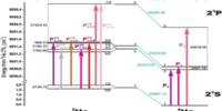
A nitrogen vacancy (NV) center in diamond is one of the most extensively studied systems due to its potential use in a wide range of quantum applications. Because the spin of NV centers is sensitive to any physical, electrical, or optical disturbance, they could be used as highly sensitive detectors. “Solid-state spin defects are one of the most promising quantum platforms,” Wang says, citing the fact that they can operate at room temperature. Many other quantum systems necessitate the use of ultracold or other specialized environments.
“NV centers’ nanoscale sensing capabilities make them promising for probing the dynamics in their spin environment, manifesting rich quantum many body physics that remains unknown,” Wang adds. “A major spin defect in the environment, called the P1 center, can usually be 10 to 100 times more populous than the NV center and thus have stronger interactions, making them ideal for studying many-body physics.”
However, in order to tune their interactions, scientists must be able to change the spin density, which has previously been difficult to achieve. “We can tune the spin density so it provides a potential knob to actually tune such a system, Wang says of this new approach. That’s the key novelty of our work.”
Such a tunable system could provide more flexible ways of studying the quantum hydrodynamics, Wang says. More immediately, the new process can be applied to some existing nanoscale quantum-sensing devices as a way to improve their sensitivity.
Li, who holds a joint appointment in MIT’s departments of Nuclear Science and Engineering and Materials Science and Engineering, explains that today’s computers and information processing systems are all based on the control and detection of electrical charges, but some innovative devices are beginning to make use of the property called spin. The semiconductor company Intel, for example, has been experimenting with new kinds of transistors that couple spin and charge, potentially opening a path to devices based on spintronics.
“Traditional CMOS transistors use a lot of energy,” Li says, “but if you use spin, as in this Intel design, then you can reduce the energy consumption by a lot.” The company has also developed solid-state spin qubit devices for quantum computing, and “spin is something people want to control in solids because it’s more energy efficient, and it’s also a carrier of quantum information.”
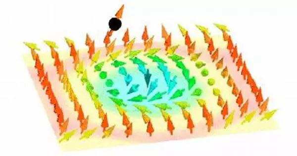
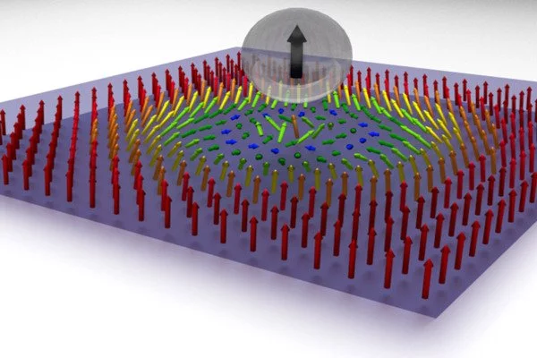
The newly achieved level of control over spin density in the study by Li and his colleagues allows each NV center to act as a kind of atomic-scale “radar” that can both sense and control the nearby spins. “Essentially, we use a specific NV defect to sense the surrounding electronic and nuclear spins.” “This quantum sensor reveals the nearby spin environment and how it is dynamically affected by the charge flow, which in this case is pumped up by the laser,” Li explains.
This system makes it possible to dynamically change the spin concentration by a factor of two, he says. This could ultimately lead to devices where a single point defect or a single atom could be the basic computational unit. “In the long run, a single point defect, and the localized spin and the localized charge on that single point defect, can be a computing logic. It can be a qubit, it can be a memory, it can be a sensor,” he says.
He adds that much work remains to develop this newly found phenomenon. “We’re not exactly there yet,” he says, but what they have demonstrated so far shows that they have “really pushed down the measurement and control of the spin and charge state of point defects to an unprecedented level. So, in the long run, I think this would support using individual defect, or a small number of defects, to become the information processing and sensing devices.”
Wang says that while “we find this phenomenon and demonstrate it,” more research is needed to fully understand the physical mechanism of what is happening in these systems. “Our next step is to delve deeper into the physics, so we can better understand what the underlying physical mechanism” is behind the effects they observe. In the long run, “we hope to explore more quantum simulation and sensing ideas, such as simulating interesting quantum hydrodynamics and even transporting quantum information between different spin defects, with a better understanding of these systems.”
The findings were made possible in part by the team’s development of a new wide-field imaging setup that allows them to simultaneously measure many different spatial locations within the crystalline material using a fast single-photon detector array and a microscope. “We are able to spatially image the density distribution over different spin species like a fingerprint, and the charge transport dynamics,” Wang says, adding that the work is still preliminary.
Although their research was conducted on lab-grown diamond, he believes the principles could be applied to other crystalline solid-state defects. Diamond NV centers have been appealing for research because they can be used at room temperature and have already been thoroughly studied. But silicon vacancy centers, donors in silicon, rare-earth ions in solids, and other crystal materials may have different properties that could turn out to be useful for particular kinds of applications.
“As information science advances, people will eventually be able to control the positions and charges of individual atoms and defects.” That is the long-term goal, according to Li. “If you can have every atom storing different information, it’s a much larger information storage and processing capability” than existing systems that store even a single bit by a magnetic domain of many atoms.You could say it’s Moore’s Law’s ultimate limit: eventually going down to one defect or one atom.”
While some applications may require much more research to develop to a practical level, Wang claims that for certain types of quantum sensing systems, new insights can be quickly translated into real-world applications. “We can immediately improve the quantum sensors’ performance based on our results,” he says.