Nickel selenide is the inorganic compound with the formula NiSe. As for many metal chalcogenides, the phase diagram for nickel(II) selenide is complicated. Two other selenides of nickel are known, NiSe2 with a pyrite structure, and Ni2Se3. Nickel selenide nanoparticles of different sizes and shapes were synthesized using a modified solvothermal method.
Additionally, NiSe is usually nonstoichiometric and is often described with the formula Ni1−xSe, with 0 < x <0.15. A one-step oleylamine-mediated solvothermal method was reported for the synthesis of nickel selenide series within a short reaction time. This material is a semi-conducting solid and can be obtained in the form of a black fine powder, or silver if obtained in the form of larger crystals. The method provided a suitable nucleation and growth environment in a uniform and transparent solution reaction system. Nickel(II) selenide is insoluble in all solvents but can be degraded by strongly oxidizing acids.
- Formula: NiSe
- Formula weight: 137.653
- Class: selenide
- Colour: pale grey or yellow-green
- Appearance: crystalline solid
- Melting point: 980°C
- Density: 7200 kg m-3
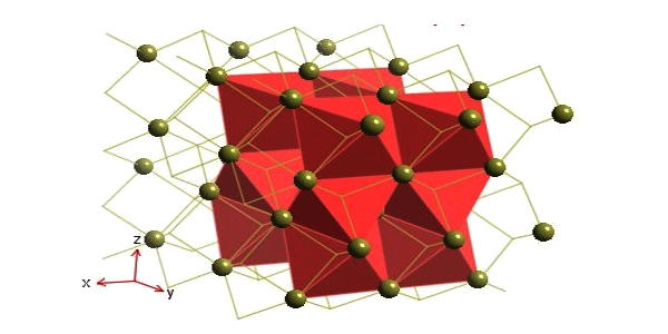
Synthesis and structure
Nickel selenide thin films have been deposited using chemical bath method on non-conducting glass substrates in a tartarate bath containing nickel sulphate octahydrate, hydrazine hydrate, sodium selenosulphate in an aqueous alkaline medium. Typically, NiSe is prepared by high temperature reaction of the elements. Such reactions typically afford mixed phase products. Milder methods have also been described using more specialised techniques such as reactions of the elements in liquid ammonia in a pressure vessel. The grown films were uniform, well adherent and black in color. The films were characterized using X-ray diffraction, scanning electron microscopy, optical absorption and electrical measurements.
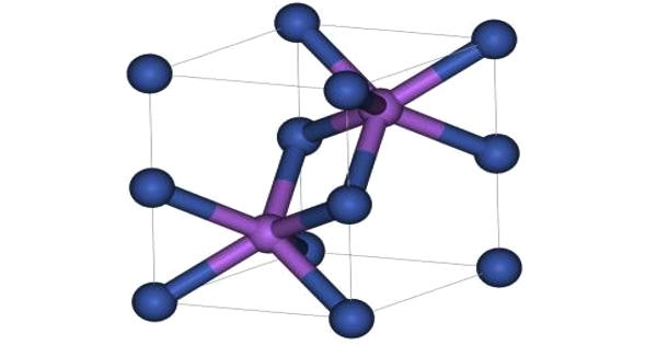
Like many related materials, nickel(II) selenide adopts the nickel arsenide motif. In this structure, nickel is octahedral and the selenides are in trigonal prismatic sites.
Uses
It is used in semiconductor, chemical vapor deposition (CVD) and physical vapor deposition (PVD) display and optical applications. It is used for coating solar energy or fuel cells and flip-chip applications.
Information Source:
