Modern data transfer, which sends data in the form of modulated light beams across fiber optic cables, is among other things based on the quick switching and modulation of light.
Engineers are still having difficulty with the light sources themselves, such as LEDs or lasers, despite years of progress in the miniaturization and chip integration of light modulators.
A team of researchers at ETH Zurich led by Prof. Lukas Novotny, together with colleagues at EMPA in Dübendorf and at ICFO in Barcelona, has now found a new mechanism by which tiny but efficient light sources could be produced in the future. The results of their research have recently been published in the journal Nature Materials.
Trying the unexpected
“To achieve this, we first had to try the unexpected,” says Novotny. For several years he and his coworkers have been working on miniature light sources that are based on the tunnel effect.
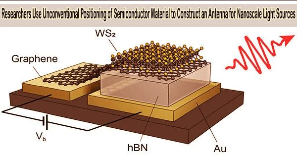
Between two electrodes (made of gold and graphene in this case) separated by an insulating material, electrons can tunnel according to the rules of quantum mechanics. Light can be produced under specific conditions, that is, if the tunnel process is inelastic, indicating that the electrons’ energy is not preserved.
“Unfortunately, the yield of those light sources is rather poor because the radiative emission is very inefficient,” explains postdoc Sotirios Papadopoulos. “This emission problem is well-known in other areas of technology. In mobile phones, for instance, the chips that create the microwaves needed for transmission are only a few millimeters in size.”
The wavelength of the microwaves, in contrast, is about 20 centimeters, making them a hundred times bigger than the chip. To overcome this difference in size an antenna is needed (which, in modern phones, is actually no longer visible from the outside). The wavelength of the light is also substantially bigger than the light source in the experiments of the Zurich researchers.
Unfortunately, the yield of those light sources is rather poor because the radiative emission is very inefficient. This emission problem is well-known in other areas of technology. In mobile phones, for instance, the chips that create the microwaves needed for transmission are only a few millimeters in size.
Sotirios Papadopoulos
Semiconductor outside the tunnel junction
“One might think, then, that we were consciously looking for an antenna solution but in reality we weren’t,” says Papadopoulos.
The researchers were looking at layers of semiconductor materials sandwiched between the electrodes of the tunnel junction with a thickness of a single atom, such as tungsten disulfide, like other groups before them.
The ideal position should, in theory, be somewhere between the two electrodes, possibly a little closer to one than the other. The semiconductor was placed on top of the graphene electrode outside the tunnel junction as an entirely new experiment by the researchers.
Surprising antenna action
Surprisingly, this apparently illogical position worked very well. By adjusting the voltage applied to the tunnel junction and observing the current flowing through it, the researchers were able to determine the cause of this. This measurement clearly demonstrated a resonance that matched the semiconductor material’s so-called exciton resonance.
Excitons are composed of an electron bonded by the positively charged hole, which stands in for a missing electron. They can be excited, for instance, by light irradiation. The exciton resonance was a definite indicator that charge carriers did not activate the semiconductor directly after all; there were no electrons passing through it.
Rather, the semiconductor had absorbed and then released the energy produced in the tunnel junction. In other words, it acted very much like an antenna.
Applications in nanoscale light sources
“For now, this antenna is not very good because inside the semiconductor so-called dark excitons are created, which means that not much light is emitted,” Novotny concedes. “Improving this will be our homework for the near future.”
It should be able to develop light sources that measure only a few nanometers and are thus a thousand times smaller than the wavelength of the light they produce if the researchers are successful in increasing the efficiency of the light emission by the semiconductor.
The semiconductor antenna doesn’t have any electrons flowing through it, so it also doesn’t have any of the undesirable effects that frequently happen at borders and can lower efficiency.
“In any case, we have opened a door to new applications,” says Novotny. Trying the unexpected has evidently paid off.