The number of transistors on a microchip has doubled annually since the 1960s, as predicted by Moore’s Law. The silicon that serves as the basis for current transistors, however, loses its electrical qualities once the size of the devices built from it drops below a certain point, therefore it is projected that this trend will soon plateau.
We now have 2D materials, which are fragile, two-dimensional sheets made of flawless crystals that are only a single atom thick. 2D materials can carry electrons far more effectively than silicon at the nanoscale scale. Therefore, 2D materials have received the majority of attention in the hunt for next-generation transistor materials that could replace silicon..
But before the electronics industry can switch to 2D materials, researchers must first figure out how to design the materials on silicon wafers that meet industrial standards while maintaining their ideal crystalline shape. And MIT engineers may now have a solution.
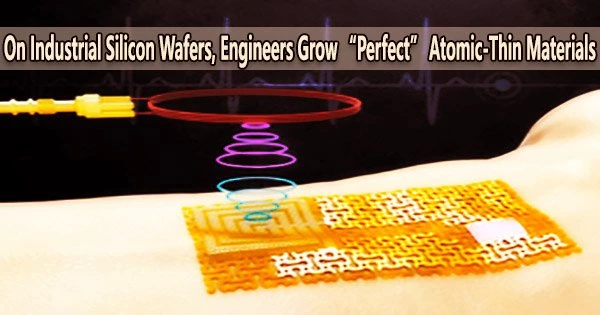
The team has created a technique that could allow chip makers to create transistors made of 2D materials that are ever thinner by growing them on silicon and other material wafers now in use. The team’s innovative technique, which they first applied to build pure, defect-free 2D materials onto industrial silicon wafers, is a type of “nonepitaxial, single-crystalline growth.”
With their method, the team fabricated a simple functional transistor from a type of 2D materials called transition-metal dichalcogenides, or TMDs, which are known to conduct electricity better than silicon at nanometer scales.
“We expect our technology could enable the development of 2D semiconductor-based, high-performance, next-generation electronic devices,” says Jeehwan Kim, associate professor of mechanical engineering at MIT. “We’ve unlocked a way to catch up to Moore’s Law using 2D materials.”
Kim and his colleagues detail their method in a paper appearing in Nature. The study’s MIT co-authors include Ki Seok Kim, Doyoon Lee, Celesta Chang, Seunghwan Seo, Hyunseok Kim, Jiho Shin, Sangho Lee, Jun Min Suh, and Bo-In Park, along with collaborators at the University of Texas at Dallas, the University of California at Riverside, Washington University in Saint Louis, and institutions across South Korea.
A crystal patchwork
Traditionally, researchers have used a manual procedure in which an atom-thin flake is meticulously exfoliated from a bulk material, similar to peeling an onion’s layers.
However, the majority of bulk materials are polycrystalline, consisting of many crystals that grow in a variety of directions. The “grain boundary” works as an electric barrier where two crystals collide. Any electrons that are passing through one crystal and encountering a crystal with a different orientation abruptly stop, dampening the conductivity of the material.
We expect our technology could enable the development of 2D semiconductor-based, high-performance, next-generation electronic devices. We’ve unlocked a way to catch up to Moore’s Law using 2D materials.
Professor Jeehwan Kim
Researchers must search a 2D flake for “single-crystalline” regions even after exfoliating it; this is a laborious and time-consuming procedure that is challenging to implement at commercial scales.
Recently, scientists have discovered more methods for creating 2D materials, including growing them on sapphire wafers, a substance having an atom structure that enables 2D materials to form in the same, single-crystalline orientation.
“But nobody uses sapphire in the memory or logic industry,” Kim says. “All the infrastructure is based on silicon. For semiconductor processing, you need to use silicon wafers.”
However, wafers of silicon lack sapphire’s hexagonal supporting scaffold. When scientists try to create 2D materials on silicon, the end result is a chaotic patchwork of crystals that randomly fuse, creating multiple grain boundaries that impede conductivity.
“It’s considered almost impossible to grow single-crystalline 2D materials on silicon,” Kim says. “Now we show you can. And our trick is to prevent the formation of grain boundaries.”
Seed pockets
The team’s new “nonepitaxial, single-crystalline growth” does not require peeling and searching flakes of 2D material. Instead, the scientists pump atoms over a silicon chip using standard vapor deposition techniques. At some point, the atoms land on the wafer, nucleate, and develop into two-dimensional crystal orientations.
Each “nucleus,” or crystal seed, would develop in a random orientation across the silicon wafer if left unattended. However, Kim and his colleagues managed to align each crystal as it grew to produce single-crystalline areas all over the wafer.
To do so, they first covered a silicon wafer in a “mask” a coating of silicon dioxide that they patterned into tiny pockets, each designed to trap a crystal seed. Then, a gas of atoms that settled into each pocket to create a 2D material in this example, a TMD, flowed across the masking wafer. The atoms were contained by the mask’s pockets, which encouraged them to group together on the silicon wafer in a single, crystalline orientation.
“That is a very shocking result,” Kim says “You have single-crystalline growth everywhere, even if there is no epitaxial relation between the 2D material and silicon wafer.”
The team created a straightforward TMD transistor using their masking technique, and they demonstrated that its electrical performance was on par with that of a pure flake of the same material.
They also applied the method to engineer a multilayered device. They first grew one kind of 2D material to fill half of each square on a silicon wafer covered in a patterned mask, then they grew another kind of 2D material over the first layer to fill the remaining squares. The result was an ultrathin, single-crystalline bilayer structure within each square.
Kim says that going forward, “multiple 2D materials could be grown and stacked together in this way to make ultrathin, flexible, and multifunctional films.”
“Until now, there has been no way of making 2D materials in single-crystalline form on silicon wafers, thus the whole community has almost given up on pursuing 2D materials for next-generation processors,” Kim says.
“Now we have completely solved this problem, with a way to make devices smaller than a few nanometers. This will change the paradigm of Moore’s Law.” This research was supported in part by DARPA, Intel, the IARPA MicroE4AI program, MicroLink Devices, Inc., ROHM Co., and Samsung.