Nanolithography is a process used in nanotechnology and semiconductor manufacturing to create nanoscale patterns or structures. It is a growing branch of nanotechnology that deals with the engineering (patterning, for example, etching, depositing, writing, printing, etc.) of nanometer-scale structures on various materials. It entails the precise manipulation and placement of materials on a substrate to form intricate patterns with features on the order of nanometers (billionths of a meter).
The primary goal of nanolithography is to create extremely small devices or components, such as integrated circuits, nanoscale sensors, or other nanostructured materials. It is possible to take advantage of quantum mechanical effects and achieve unique properties or enhanced performance in a variety of applications by creating patterns on such a small scale.
In nanolithography, several techniques are used, each with its own set of advantages and disadvantages. Here are a few commonly used methods:
- Optical Lithography: Light is used to transfer a pattern from a mask or photomask to a photosensitive material, typically a photoresist. It has been widely used in semiconductor manufacturing, but it is limited by light diffraction, preventing further feature size reduction beyond a certain limit.
- Electron Beam Lithography (EBL): EBL employs a focused electron beam to directly write patterns on a substrate. Magnetic lenses are used to control the electron beam, allowing for precise positioning and control. It has a high resolution and flexibility but is time consuming for large-scale patterning.
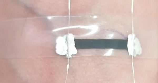
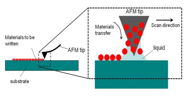
- Scanning Probe Lithography: This technique involves using a sharp probe, such as an atomic force microscope (AFM) or scanning tunneling microscope (STM), to directly write or modify patterns on a substrate. It offers high resolution and the ability to work with a variety of materials, but it is generally a slow process.
- Nanoimprint Lithography: Nanoimprint lithography uses a rigid mold or stamp with the desired pattern, which is pressed into a thermoplastic material to transfer the pattern. It can achieve high resolution and high throughput but may have challenges with mold fabrication and defect control.
- Extreme Ultraviolet Lithography (EUV): EUV lithography transfers patterns from a mask to a substrate by using very short-wavelength light in the extreme ultraviolet range. It can produce smaller features than optical lithography and has been used in advanced semiconductor manufacturing.
The modern term refers to structures built in the range of 109 to 106 meters, i.e. on a nanometer scale. Essentially, the field is a subset of lithography that only deals with very small structures. All NL methods can be divided into four categories: photolithography, scanning lithography, soft lithography, and other techniques.