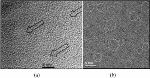
Nanocrystalline silicon (nc-Si), also known as microcrystalline silicon (c-Si), is a porous silicon material. It is a type of silicon composed of tiny crystalline structures on the nanometer scale, typically ranging in size from 1 to 100 nanometers. It is an allotropic form of silicon with a paracrystalline structure that, like amorphous silicon (a-Si), has an amorphous phase. These nanocrystals are much smaller than traditional polycrystalline silicon crystals. The difference is that nc-Si contains small grains of crystalline silicon within the amorphous phase. In contrast, polycrystalline silicon (poly-Si) is made up entirely of crystalline silicon grains separated by grain boundaries.
The only difference is the grain size of the crystalline grains. Because most materials with grains in the micrometre range are fine-grained polysilicon, the term nanocrystalline silicon is more appropriate. The term nanocrystalline silicon refers to a variety of materials found in the silicon thin film near the transition region from amorphous to microcrystalline phase. Another criterion for describing the materials in this transition zone is the crystalline volume fraction (as measured by Raman spectroscopy).
This unique structure imparts various properties and potential applications to nanocrystalline silicon:
- Optical Properties: The optical properties of nanocrystalline silicon, such as quantum confinement effects, are fascinating. When nanocrystals are small enough, they can emit light at various wavelengths based on their size. This property has applications in optoelectronic devices such as LEDs and photodetectors.
- Electronic Properties: The electronic properties of nanocrystals can also be influenced by their size. Small nanocrystals with discrete energy levels can be used in quantum dots and other nanoscale electronic components.
- Increased Surface Area: Because of the presence of many small crystals, nanocrystalline materials have a large surface area. As a result, they can be used in a variety of applications, including sensors, catalysis, and energy storage devices.
- Improved Solar Cells: Nanocrystalline silicon has been explored for use in photovoltaic cells. Its unique properties can enhance the absorption of light and improve the efficiency of solar cells.
- Thin-Film Technology: Nanocrystalline silicon can be used to create thin films for various applications, including in displays, sensors, and electronic components. These thin films can be deposited on flexible substrates, making them suitable for flexible electronics.
Because of their biocompatibility and ability to transport drugs or contrast agents to specific targets, nanocrystalline silicon nanoparticles can be used in biomedical applications such as drug delivery and imaging. It’s also been looked into for use in lithium-ion batteries. Its large surface area can improve the performance of the electrode and increase its energy storage capacity.
Advantages
Because of the presence of silicon crystallites, nc-Si has many useful advantages over a-Si, one of which is that it can have higher electron mobility if grown properly. It also absorbs more in the red and infrared wavelengths, making it an important material for use in a-Si solar cells.
One of the most significant advantages of nanocrystalline silicon over a-Si is its increased stability, which is due in part to its lower hydrogen concentration. Although it cannot currently achieve the mobility of poly-Si, it has the advantage of being easier to fabricate than poly-Si because it can be deposited using conventional low temperature a-Si deposition techniques, such as PECVD, as opposed to laser annealing or high temperature CVD processes in the case of poly-Si.