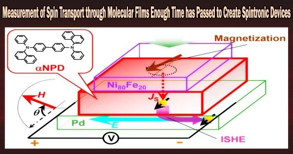
Spin transport, also known as “spin transport phenomena,” refers to the movement of spin-carrying charge carriers, such as electrons, through a material. The measurement of spin transport through molecular films has recently advanced to the point where the films are long enough to potentially be used in the development of spintronic devices.
A study team has been successful in monitoring the spin transfer in a thin film of certain molecules, a substance commonly used in organic light-emitting diodes. They discovered that the spin diffusion length of this thin molecular film is roughly 62 nm, a length that may be useful for creating spintronics technology.
Additionally, the thin molecular layer utilized in this study is photoconductive, allowing spin transport control using visible light, whereas in the past electricity has been used to control spin transport.
Because of improvements in microfabrication technology, information processing devices like smartphones are getting more complex due to a steady increase in information recording density.
Recent years, however, have seen a rapid approach of the processing’s physical constraints, making further downsizing challenging. However, it’s possible that the ongoing need for more advanced technology necessitates a fundamental shift in operating theories, allowing for the continual production of quicker, smaller, and newer devices.
For practical use, it will be necessary to uncover more details about spin injection and spin transport mechanisms through thin molecular films to control spin transport. Further research is expected to lead to the realization of super energy-efficient devices that use small amounts of power and have little risk of overheating.
Professors Eiji Shikoh
The next generation of sophisticated electronics may be unlocked by a technology known as spintronics, which uses the magnetic spin and charge of electrons to meet this requirement. It is feasible to spread information using very little power and produce less waste heat by aligning a magnetic spin’s direction and moving it like an electric current.
A research group, led by Professors Eiji Shikoh and Yoshio Teki of the Osaka Metropolitan University Graduate School of Engineering, has successfully measured spin transport, at room temperature, in a thin film of alpha-naphthyl diamine derivative (NPD) molecules, a well-known material in organic light emitting diodes. They discovered that this molecular thin film had a spin diffusion length of roughly 62 nanometers, a length that they anticipate can be exploited in real-world scenarios.
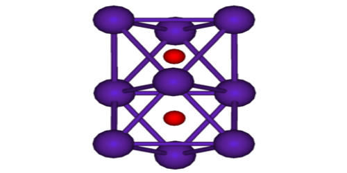
It is necessary to have a spin diffusion length in the tens of nanometer range at room temperature for precise processing in order to leverage spin transport to create spintronics technology. Thermal evaporation in vacuum was used to create the thin molecular film of NPD for this work, which has a spin diffusion length of 62 nanometers, a significant distance for molecular materials.
Previously, spin transport was controlled by electricity, but the new thin NPD molecular film is photoconductive, allowing spin transport to be controlled by visible light.
“For practical use, it will be necessary to uncover more details about spin injection and spin transport mechanisms through thin molecular films to control spin transport,” noted Professor Shikoh. “Further research is expected to lead to the realization of super energy-efficient devices that use small amounts of power and have little risk of overheating.”
Spintronics is a field of study that combines the principles of electronics and spin to create new types of devices with unique functionality. The successful measurement of spin transport through molecular films is an important step in the development of this field and could lead to the creation of new, more efficient and versatile devices.