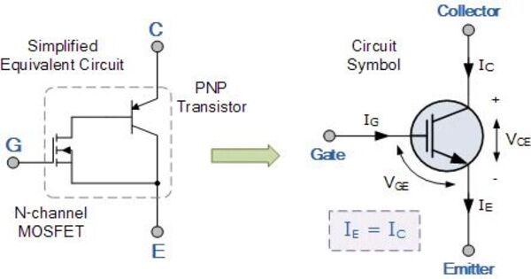
An insulated-gate bipolar transistor (IGBT) is a three-terminal power semiconductor that functions primarily as an electronic switch. It is a semiconductor device that is widely used in power electronics for switching and amplification purposes. It was designed to combine high efficiency and quick switching. It is made up of four alternating layers (P-N-P-N), which are controlled by a metal-oxide-semiconductor gate arrangement. It combines the greatest features of both metal oxide semiconductor field-effect transistors (MOSFETs) and bipolar junction transistors (BJTs).
Although the structure of the IGBT is topologically similar to a thyristor with a “MOS” gate (MOS-gate thyristor), the thyristor action is totally suppressed, and only the transistor action is permitted throughout the device’s operating range. It is used in high-power switching power supplies such as variable-frequency drives (VFDs) for motor control in electric cars, trains, variable-speed refrigerators, and air conditioners, as well as lamp ballasts, arc welding machines, uninterruptible power supply systems (UPS), and induction stoves.
Key Features
- High Efficiency: IGBTs can handle high voltages and currents with high efficiency, making them suitable for high-power applications.
- Fast Switching: They offer fast switching capabilities, although not as fast as MOSFETs. This makes them suitable for applications where switching speed is critical but not the utmost priority.
- Voltage Control: The gate of an IGBT is voltage-controlled, similar to a MOSFET, which means it requires less power to operate compared to the current-controlled BJTs.
- High Input Impedance: The insulated gate provides a high input impedance, which reduces the power required to drive the IGBT.
- Latch-up Free: Unlike BJTs, IGBTs are latch-up free, making them more stable and reliable in operation.
Structure and Operation
- Structure: An IGBT has a four-layer structure with three terminals: the gate (G), collector (C), and emitter (E). The layers are typically N+ (drain), P (body), N- (drift region), and P+ (emitter).
- Operation: When a positive voltage is applied to the gate relative to the emitter, an inversion layer is formed, allowing current to flow from the collector to the emitter. This is similar to how a MOSFET operates, but the presence of the P+ layer gives it the high current handling capability of a BJT.
Applications
IGBTs are widely used in various applications, including:
- Power Inverters: For converting DC to AC power, such as in solar inverters, motor drives, and uninterruptible power supplies (UPS).
- Electric Vehicles: In the power electronics systems of electric and hybrid vehicles.
- Motor Control: For industrial motor drives, where efficient and reliable control of high-power motors is required.
- HVDC Systems: High-voltage direct current power transmission systems.
- Switch-Mode Power Supplies (SMPS): For efficient power conversion in various electronic devices.
Advantages
- High Voltage and Current Handling: IGBTs can handle higher voltages and currents than MOSFETs, making them suitable for high-power applications.
- Efficient Power Control: They offer efficient control with lower power losses compared to BJTs.
- Thermal Stability: Better thermal performance and stability under high-load conditions.
Disadvantages
- Switching Speed: Slower than MOSFETs, which can be a limitation in very high-frequency applications.
- Complex Drive Circuits: Requires careful design of the gate drive circuitry to avoid issues like gate charge and Miller capacitance effects.
IGBTs are a crucial component in modern power electronics, providing a balance between the fast switching of MOSFETs and the high-current handling capabilities of BJTs. They are essential for applications requiring efficient, high-power control, and their design and operation continue to evolve to meet the demands of modern technology.