City University of Hong Kong (CityU) academics lead a collaborative team that recently developed a novel technique for producing high-quality, semiconducting nanomesh at a lower temperature and cheaper cost than traditional approaches. The discoveries will make it possible to produce nanomesh for future electronics on a huge scale.
Nanomesh is a nano-scale material formed from a network of nanowires. Since they have properties like mechanical flexibility, energy efficiency, and optical transparency, one-dimensional materials like nanowires constructed of crystalline inorganic materials have been extensively researched as the major driver for developing electronics.
Nanowire semiconductors have the promise for large-area electrical and optoelectronic applications, but their scalability, integrability, and cost-effectiveness are insufficient.
By developing a low-temperature vapor-phase growing technique, a research team lead by CityU scientists overcame these drawbacks and produced semiconducting tellurium (Te) nanomesh for use in devices on a wide scale.
“The use of tellurium nanomesh in electronics holds great promise for meeting the emerging technological demands of today’s Internet of Things (IoT) applications. The progress made in this research marks a significant step towards the large-scale production of functional tellurium nanomesh, enabling potential applications that are not achievable through other means,” said Professor Johnny Ho Chung-yin, Associate Head and Professor in the Department of Materials Science and Engineering (MSE) at CityU, who led the study.
All the obtained device metrics are on par with state-of-the-art devices, but can be produced at a lower cost. They are promising for meeting emerging technological demands. This latest development has improved the transport and photoelectric properties of nanomesh and resolved concerns about the compatibility between the target device substrate and the nanomesh growth process. As a result, devices can now be produced on a wide range of technologically functional surfaces in a scalable and cost-effective manner.
Professor Johnny Ho Chung-yin
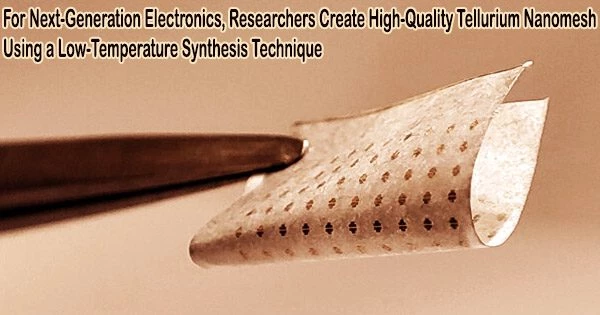
The newly created technique is capable of producing high-quality tellurium nanomesh on numerous substrates, such as silicon oxide, polymers (stretchable plastics), and even paper, in a scalable and economical manner. The findings were published in the journal Nature Communications under the title “Van der Waals nanomesh electronics on arbitrary surfaces.”
Tellurium source powders were heated at 100°C with an argon gas flow to begin the growth process. Tellurium source powders were first vaporized and transported to growth substrates.
The research team successfully produced nanomeshes made of self-assembled and self-welding tellurium nanowires laterally vapor-grown on arbitrary surfaces at the low temperature of 100°C, which is not possible using conventional methods. This novel synthesis method was designed using the principle of multi-scale van der Waals interactions of the materials.
The production cost is lower because a considerably lower temperature than usual is needed and a variety of substrates can be used to generate the nanomesh. For enhancing device performance and guaranteeing the mechanical resilience of flexible electronics, the study’s discovery of a self-welding process in the formation of tellurium nanomesh is also essential.
The team’s experiments showed how tellurium nanomesh can be used for a variety of purposes, such as micrometer-level patterning, the creation of high-mobility transistors, and the rapid and sensitive infrared photodetectors (photoresponse time under 3 microseconds) on paper.
“All the obtained device metrics are on par with state-of-the-art devices, but can be produced at a lower cost. They are promising for meeting emerging technological demands,” said Professor Ho.
“This latest development has improved the transport and photoelectric properties of nanomesh and resolved concerns about the compatibility between the target device substrate and the nanomesh growth process. As a result, devices can now be produced on a wide range of technologically functional surfaces in a scalable and cost-effective manner.”