2D perovskite structures refer to a class of materials that have the same crystal structure as the 3D perovskite mineral, but in a two-dimensional form. The 2D perovskites are a type of layered hybrid organic-inorganic compounds and are composed of inorganic cations, such as lead or tin, and organic anions, such as methylammonium or formamidinium.
Rice University researchers already knew the atoms in perovskites react favorably to light. Now they can see precisely how those atoms move.
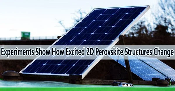
They are trying to get as much use as they can out of perovskite-based materials, such as solar cells, and a breakthrough in visualization helps them do so. This is a long-running experiment that has just lately made solar cells much more durable.
The first direct measurement of structural dynamics in 2D perovskites under light-induced excitation is described in a paper published in Nature Physics. Layered substances known as perovskites contain crystal lattices that are well-organized. They are being investigated for application as solar cells, photodetectors, photocatalysts, light-emitting diodes, quantum emitters, and other light-harvesting devices because of their high efficiency.
“The next frontier in light-to-energy conversion devices is harvesting hot carriers,” said Rice University’s Aditya Mohite, a corresponding author of the study. “Studies have shown that hot carriers in perovskite can live up to 10–100 times longer than in classical semiconductors. However, the mechanisms and design principles for the energy transfer and how they interact with the lattice are not understood.”
Hot carriers are short-lived, high-energy charge carriers, either electrons for negative charges or electron “holes” for positive charges, and having the ability to harvest their energy would allow light-harvesting devices to “surpass thermodynamic efficiency,” said Mohite, an associate professor of chemical and biomolecular engineering in Rice’s George R. Brown School of Engineering.
Studies have shown that hot carriers in perovskite can live up to 10–100 times longer than in classical semiconductors. However, the mechanisms and design principles for the energy transfer and how they interact with the lattice are not understood.
Aditya Mohite
Mohite and three members of his research group, senior scientist Jean-Christophe Blancon and graduate students Hao Zhang and Wenbin Li, worked with colleagues at the SLAC National Accelerator Laboratory to see how atoms in a perovskite lattice rearranged themselves when a hot carrier was created in their midst. They visualized lattice reorganization in real time using ultrafast electron diffraction.
“Whenever you expose these soft semiconductors to stimuli like electric fields, interesting things happen,” Mohite said. “When you generate electrons and holes, they tend to couple to the lattice in unusual and really strong ways, which is not the case for classical materials and semiconductors.”
“So there was a fundamental physics question,” he said. “Can we visualize these interactions? Can we see how the structure is actually responding at very fast timescales as you put light onto this material?”
Yes, but only with a significant input, was the response. One of the few locations in the world with pulsed lasers capable of producing the electron-hole plasma in perovskites that was required to reveal how the lattice structure changed in less than a billionth of a second in response to a hot carrier is SLAC’s mega-electron-volt ultrafast electron diffraction (MeV-UED) facility.
“The way this experiment works is that you shoot a laser through the material and then you send an electron beam that goes past it at a very short time delay,” Mohite explained. “You start to see exactly what you would in a TEM (transmission electron microscope) image. With the high-energy electrons at SLAC, you can see diffraction patterns from thicker samples, and that allows you to monitor what happens to those electrons and holes and how they interact with the lattice.”
The team led by Mohite evaluated the before-and-after diffraction patterns from the SLAC tests to demonstrate how the lattice evolved. They discovered that the lattice physically straightened up in as little as one picosecond, or one trillionth of a second, after being activated by light.
Zhang said, “There’s a subtle tilting of the perovskite octahedra, which triggers this transient lattice reorganization towards a higher symmetric phase.”
The research indicated it should be able to regulate how perovskite lattices interact with light, and it offered a mechanism to do the tuning by proving that a perovskite lattice can abruptly become less distorted in reaction to light.
Li said, “This effect is very dependent on the type of structure and type of organic spacer cation.”
There are numerous methods for creating perovskites, but each one calls for the addition of organic cations, which serve as a divider between the semiconducting layers. By substituting or subtly changing organic cations, researchers could tailor lattice rigidity, dialing it up or down to alter how the material responds to light, Li said.
Mohite said the experiments also show that tuning a perovskite’s lattice alters its heat-transfer properties.
“What is generally expected is that when you excite electrons at a very high energy level, they lose their energy to the lattice,” he said. “Some of that energy is converted to whatever process you want, but a lot of it is lost as heat, which shows in the diffraction pattern as a loss in intensity.”
“The lattice is getting more energy from thermal energy,” Mohite said. “That’s the classical effect, which is expected, and is well-known as the Debye-Waller factor. But because we can now know exactly what’s happening in every direction of the crystal lattice, we see the lattice starts to get more crystalline or ordered. And that’s totally counterintuitive.”
“A better understanding of how excited perovskites handle heat is a bonus of the research,” he said.
“As we make devices smaller and smaller, one of the biggest challenges from a microelectronics perspective is heat management,” Mohite said. “Understanding this heat generation and how it’s being transported through materials is important.”
“When people talk about stacking devices, they need to be able to extract heat very fast,” he said. “As we move to new technologies that consume less power and generate less heat, these types of measurements will allow us to directly probe how heat is flowing.”