Because quantum systems are inherently susceptible to errors due to factors such as decoherence and noise, quantum error correction (QEC) is a critical aspect of quantum computing. Scientists have trapped electrons in a pure crystal, achieving the first electronic flat band in a three-dimensional material. The findings open up new avenues for scientists to investigate rare electronic states in 3D materials.
Electrons move through a conducting material like commuters during rush hour in Manhattan. The charged particles may jostle and bump against one another, but they’re mostly unconcerned with other electrons as they hurtle forward, each with their own energy.
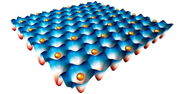
When electrons in a material are trapped together, they can settle into the same energy state and begin to behave as one. This collective, zombie-like state is referred to in physics as an electronic “flat band,” and scientists predict that electrons in this state will begin to feel the quantum effects of other electrons and will act in coordinated, quantum ways. Exotic phenomena such as superconductivity and novel forms of magnetism may then emerge.
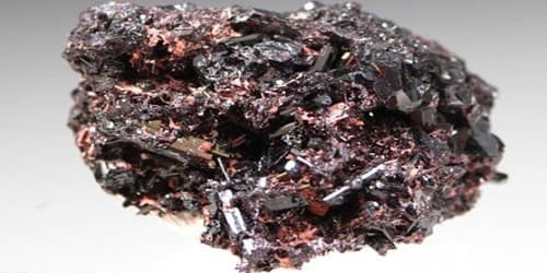
MIT physicists have succeeded in trapping electrons in a pure crystal. Scientists have created an electronic flat band in a three-dimensional material for the first time. The researchers also demonstrated that with some chemical manipulation, they could convert the crystal into a superconductor – a material that conducts electricity with zero resistance.
For this experiment, you typically require a very flat surface. However, the surface of these 3D materials resembles the Rocky Mountains, with a very corrugated landscape. Experiments on these materials are extremely difficult, which is why no one has demonstrated that they host trapped electrons.
Riccardo Comin
The trapped state of the electrons is made possible by the crystal’s atomic geometry. The physicists created a crystal with an atom arrangement that resembles the woven patterns in “kagome,” the Japanese art of basket weaving. The researchers discovered that rather than jumping between atoms, electrons were “caged,” and settled into the same energy band.
The researchers say that this flat-band state can be realized with virtually any combination of atoms — as long as they are arranged in this kagome-inspired 3D geometry. The results, appearing in Nature, provide a new way for scientists to explore rare electronic states in three-dimensional materials. These materials might someday be optimized to enable ultra-efficient power lines, supercomputing quantum bits, and faster, smarter electronic devices.
“Now that we know we can make a flat band from this geometry, we have a big motivation to study other structures that might have other new physics that could be a platform for new technologies,” says study author Joseph Checkelsky, associate professor of physics.
Checkelsky’s MIT co-authors include graduate students Joshua Wakefield, Mingu Kang, and Paul Neves, and postdoc Dongjin Oh, who are co-lead authors; graduate students Tej Lamichhane and Alan Chen; postdocs Shiang Fang and Frank Zhao; undergraduate Ryan Tigue; associate professor of nuclear science and engineering Mingda Li; and associate professor of physics Riccardo Comin, who collaborated with Checkelsky to direct the study; along with collaborators at multiple other laboratories and institutions.
Setting a 3D trap
Physicists have successfully trapped electrons and confirmed their electronic flat-band state in two-dimensional materials in recent years. However, scientists have discovered that electrons trapped in two dimensions can easily escape into the third, making flat-band states difficult to maintain in two dimensions.
Checkelsky, Comin, and their colleagues set out to create flat bands in three-dimensional materials so that electrons could be trapped in all three dimensions and exotic electronic states could be more stably maintained. They suspected that kagome patterns might be involved.
Previously, the team discovered trapped electrons in a two-dimensional atom lattice that resembled some kagome designs. Instead of hopping across the lattice, electrons were confined within the hexagonal space between triangles when the atoms were arranged in a pattern of interconnected, corner-sharing triangles. However, the researchers discovered, like others, that electrons could escape up and out of the lattice via the third dimension.
Could a 3D configuration of similar lattices work to contain the electrons? They looked for an answer in material structure databases and came across a specific geometric configuration of atoms, which was classified as a pyrochlore – a type of mineral with highly symmetric atomic geometry. The pychlore’s 3D structure of atoms formed a repeating pattern of cubes, the face of each cube resembling a kagome-like lattice. They found that, in theory, this geometry could effectively trap electrons within each cube.
Rocky landings
To test this hypothesis, the researchers synthesized a pyrochlore crystal in the lab.
“It’s not dissimilar to how nature makes crystals,” Checkelsky explains. “We put certain elements together — in this case, calcium and nickel — melt them at very high temperatures, cool them down, and the atoms on their own will arrange into this crystalline, kagome-like configuration.”
They then looked to measure the energy of individual electrons in the crystal, to see if they indeed fell into the same flat band of energy. To do so, researchers typically carry out photoemission experiments, in which they shine a single photon of light onto a sample, that in turn kicks out a single electron. A detector can then precisely measure the energy of that individual electron.
Photoemission has been used by scientists to confirm flat-band states in various 2D materials. Because they are physically flat and two-dimensional, these materials are relatively easy to measure with standard laser light. The task is more difficult for 3D materials.
“For this experiment, you typically require a very flat surface,” Comin goes on to explain. “However, the surface of these 3D materials resembles the Rocky Mountains, with a very corrugated landscape.” Experiments on these materials are extremely difficult, which is why no one has demonstrated that they host trapped electrons.”
This obstacle was overcome by the team using angle-resolved photoemission spectroscopy (ARPES), an ultrafocused beam of light capable of targeting specific locations across an uneven 3D surface and measuring the individual electron energies at those locations.
“It’s like landing a helicopter on very small pads, all across this rocky landscape,” Comin said.
The team used ARPES to measure the energies of thousands of electrons across a simulated crystal sample in about half an hour. They discovered that the electrons in the crystal all had the same energy, confirming the flat-band state of the 3D material.
The researchers created the same crystal geometry, but this time with atoms of rhodium and ruthenium instead of nickel, to see if they could manipulate the coordinated electrons into some exotic electronic state. On paper, the researchers calculated that this chemical swap would shift the electrons’ flat band to zero energy, resulting in superconductivity.
When they synthesized a new crystal with a slightly different combination of elements in the same kagome-like 3D geometry, they discovered that the crystal’s electrons exhibited a flat band, this time at superconducting states.