Since the creation of the world’s first transistor by Bell Labs researchers in December 1947, a revolution in microelectronics technology has had a significant impact on lives all over the world. It is difficult to discover a simple, quick, and affordable method of fabricating micro-nano components as electronics become smaller and smaller.
Mechanical scribing, focused ion beam etching, electron beam lithography, multiphoton polymerization, and thermal scanning probe etching are examples of conventional direct writing fabrication techniques that are ineffective.
Although techniques like nanoimprinting, photolithography, plasma etching, and scanning laser interference etching can significantly speed up processing, they frequently involve multiple steps, such as the creation of masks, or they call for extremely harsh working conditions and depend on specialized materials.
Attention has been drawn to the creation of nanograting structures by inducing surface self-organized periodic structure with a femtosecond laser. Laser-induced periodic surface structures (LIPSS) provide great processing accuracy because they erode the material using the interference of incident light and surface electromagnetic waves.
Additionally, the self-organized processing method’s experimental setup is simpler and its manufacturing speed is rapidly high when compared to the conventional laser interference processing method.
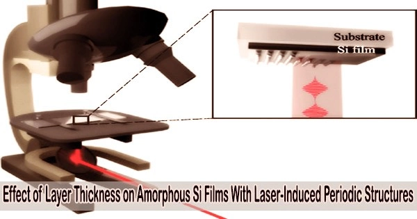
Researchers led by Prof. Min Qiu at Westlake University, China have extensive research experience in LIPSS. They recently found that when a periodic grating is produced on the surface of a thin a-Si film, the interference of incident light with various electromagnetic wave sources affects the grating’s period.
Their paper, “Impact of film thickness in laser-induced periodic structures on amorphous Si films” has been published in Frontiers of Optoelectronics.
LIPSS with a short period is induced when the slab waveguide mode predominates and the substrate is made of a non-silicon material and the amorphous silicon film is just 50 nm thick. In this case, when the substrate material changes (refractive index changes), the period of the LIPSS also changes.
The incident light interferes with the quasi-cylindrical wave and causes the formation of LIPSS under the combined action of near-field and far-field when the thickness of the amorphous silicon film is substantial (200 nm).
The period of LIPSS in this mode is independent of the substrate material and is just a little bit shorter than the laser wavelength. Numerical simulations based on the finite-difference time-domain approach support the results of the experiments.